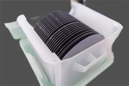
| Crystal structure | face centered cubic | | | ||
| Melting point (°C) | 1420 | | | ||
| Density | 2.4 (g/cm 3 ) | | | ||
| Doping substance | Not adulterated | Doped with B | Doped with P | ||
| Type | I | P | N | ||
| Resistivity | Ø 1000Ωcm | 10-3~40Ωcm | 10-3~40Ωcm | ||
| EPD | ≤100 cm2 | ≤100 cm2 | ≤100 cm2 | ||
| Oxygen content (cm3) | ≤1~1.8×10 18 | ≤1~1.8×10 18 | ≤1~1.8×10 18 | ||
| Carbon content (cm3) | ≤5×10 16 | ≤5×10 16 | ≤5×10 16 | ||
| Dimensions ( mm ) | 10×3, 10×5, 10×10, 15×15 , 2/3/4 inches, etc. Dia50.8mm, Dia76.2mm, Dia100mm Substrates with special directions and sizes can be customized according to customer needs | | | ||
| Thickness | 0.5mm, 1.0mm | | | ||
| Dimensional tolerance | ±0.1mm | | | ||
| Thickness Tolerance | <±0.015mm special requirements can reach <±0.005mm) | | | ||
| Polishing | single or double sided | | | ||
| Orientation Accuracy of Crystal Plane | ±0.5° | | | ||
| Edge Orientation Accuracy | 2° (special requirements can reach within 1°) | | | ||
| Orientation | <100>, <110>, <111>, etc. | | | ||
| Package | Class 100 clean bag, Class 1000 ultra-clean room | | | ||